Wafer flatness inspection is performed to verify that semiconductor wafers remain within specified flatness tolerances by measuring the surface profile relative to a reference plane. Throughout semiconductor manufacturing, the wafer may bend or warp as it undergoes different processing steps.
Maintaining wafer flatness is essential to ensure process consistency during subsequent manufacturing stages. Excessive surface curvature can affect subsequent manufacturing processes, potentially reducing manufacturing yield and product quality.
Our ISO/IEC 17025 accredited CMM measurement services provide accurate and traceable flatness measurements to verify compliance with customer specifications.
Measurement Requirements
Two semiconductor wafers were measured to verify compliance with the specified flatness requirements. The objective was to evaluate the front and back surfaces against the customer's specified flatness tolerance.
Measurement Setup
Two semiconductor wafers were performed on our Accretech AXCEL RDS 9/10/6 at our Metrology Application Centre (MAC) under our ISO/IEC 17025 accredited CMM measurement service. All measurements were carried out under controlled environmental conditions at a temperature of 20.0 to 21.0°C and a relative humidity of 50 to 60%.
Execution
Each wafer was securely mounted using a customer-provided fixture to ensure stable positioning throughout the inspection.
The front surface of each wafer was measured automatically with approximately 2,000 probing points, providing a high-density representation of the surface profile.
To minimise edge effects, probing locations were distributed uniformly across the wafer surface and positioned approximately 2mm inward from the wafer edge, as illustrated in Figure 1 below.
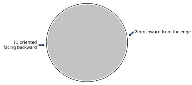
Figure 1
Results and Benefits
The measurements generated detailed three-dimensional surface profiles of both the front and back surfaces of each wafer, providing comprehensive data for accurate flatness evaluation.
The resulting colour maps clearly illustrate variations in surface height relative to the zero reference plane, allowing overall wafer curvature and localised surface deviations to be identified. The table below summarises the measured flatness values for both wafers against the specified limit range of 1.000mm. Representative front measurements can be seen in Figure 2 below.
|
Part Number
|
Front Flatness (mm)
|
Back Flatness (mm)
|
|
Part 1
|
0.95603
|
1.21353
|
|
Part 2
|
0.99588
|
1.15913
|
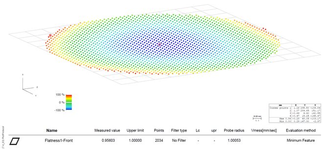
Figure 2
The inspection results showed that flatness varied between the front and back surfaces of the three wafers, enabling the customer to identify wafers that met the required flatness specification and those requiring further evaluation.
Our ISO/IEC 17025 accredited CMM measurement service provides reliable and traceable measurement results to support quality verification across a wide range of applications. Using calibrated equipment and established measurement procedures, manufacturers can verify compliance with specifications, support process validation, reduce measurement uncertainty, and maintain consistent product quality.